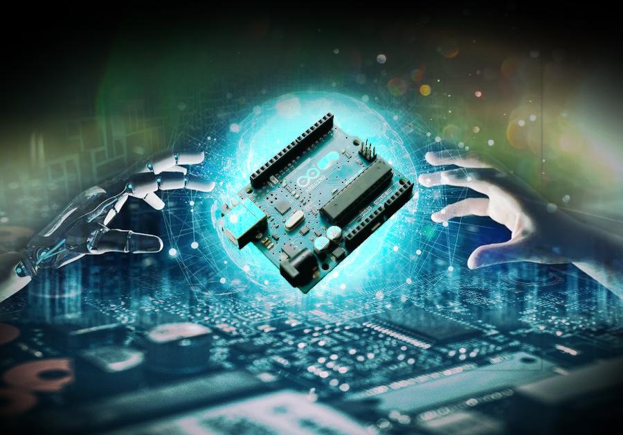
Printed Circuit Boards (PCBs) are the backbone of modern electronics, serving as the foundation for all electronic devices. From smartphones to medical equipment, PCBs play a pivotal role in connecting components and enabling the seamless functionality of intricate electronic systems. The journey from designing a PCB to obtaining a fully functional finished product involves a series of carefully orchestrated steps known as PCB assembly. In this article, we’ll demystify the process of PCB assembly, breaking down the stages from design to the creation of a polished finished product.
Design Phase: The Blueprint for Success
The journey of PCB assembly starts with the design phase. Engineers work closely with CAD software to create a virtual representation of the PCB layout. This design includes the arrangement of components, their connections, and the traces that form the electrical pathways. Design considerations such as signal integrity, power distribution, and thermal management are crucial at this stage to ensure optimal performance and reliability.
Component Procurement: Sourcing the Puzzle Pieces
Once the design is complete, the next step is to procure the components. These components range from resistors and capacitors to microprocessors and connectors. Manufacturers must carefully select components based on factors like availability, quality, and compatibility with the design. Often, components are sourced from a variety of suppliers to ensure a steady supply chain.
PCB Fabrication: Bringing the Design to Life
With the components in hand, it’s time to fabricate the actual PCB. This involves transferring the design onto a physical board using specialized techniques like etching or additive manufacturing. The PCB fabrication process demands precision, as even minor errors can lead to functionality issues down the line. During this phase, the copper traces are laid out, vias are added, and solder mask layers are applied.
Solder Paste Application: Where Components Find Their Home
To attach components to the PCB, solder paste is applied to designated areas. Solder paste is a mixture of small solder particles and flux. The flux helps clean the surfaces and enables a solid solder joint during the reflow process. This paste is applied using stencils that match the layout of the components. The paste is carefully deposited onto the PCB, ready to host the components in their precise positions.
Component Placement: The Art of Precision
With solder paste in place, the components are precisely placed onto their designated spots on the PCB. Automated assembly machines use cameras and algorithms to ensure accurate placement. This step requires extreme precision, as even the slightest misalignment can result in faulty connections or non-functional components. Once placed, the components adhere to the solder paste, holding them in position until the soldering process.
Reflow Soldering: Fusing Components Together
Reflow soldering is a critical step that involves heating the PCB to melt the solder paste and fuse the components onto the board. This process is often executed in specialized ovens with controlled temperature profiles. As the solder paste melts, it forms strong connections between the components and the PCB. The cooling phase solidifies the solder joints, creating durable connections that withstand operational stresses.
Testing and Inspection: Ensuring Quality
After soldering, the PCB undergoes thorough testing and inspection to ensure quality and functionality. Automated tests and visual inspections are performed to identify any manufacturing defects, like shorts or open circuits. Advanced techniques such as X-ray imaging can be used to examine hidden solder joints and intricate components. Any issues detected are corrected before moving forward.
Final Assembly: Completing the Puzzle
With the components securely soldered, the PCB undergoes final assembly. This may involve attaching connectors, mounting the PCB within an enclosure, and integrating any external components like buttons or displays. This stage brings the PCB assembly closer to the finished product, ready to be powered up and tested for its intended purpose.
Functional Testing: Validating Performance
Before the PCB assembly can be deemed complete, it must undergo functional testing. This involves powering up the device and running tests to ensure that all components are functioning as intended. Engineers verify that signals are passing correctly, power is distributed appropriately, and any firmware or software components are running smoothly. This stage identifies any last-minute issues that need addressing.
Packaging and Distribution: Ready for the World
Once the PCB assembly passes all tests, it’s time for packaging and distribution. The finished product is carefully packaged to protect it during transportation and storage. Documentation, user manuals, and any necessary accessories are included in the package. The product is then distributed to retailers, customers, or integrated into larger systems, ready to serve its intended purpose.
Evolute Cleantech Solutions is not only making significant advancements in the realm of Electronic Manufacturing Solutions but also serves a diverse range of industries, encompassing Fintech, Cleantech, retail, transit, medical, automotive, and more.
Our expertise includes:
Operating an in-house SMT Line boasting a remarkable 65,000 CPH capacity, furnished with cutting-edge equipment such as:
- Automatic Solder Paste Printer
- Two Pick & Place Machines
- Automatic Reflow Oven
- Automatic Optical Inspection (AOI)
- BGA Rework Station
- X Ray Inspection
This state-of-the-art facility adeptly manages complex assemblies featuring components as compact as 0201 BGA and Micro BGA. Furthermore, we’re committed to doubling our capacity within the next three months.
We’ve prioritized process automation, effectively integrating ERP as an accounting system for optimum execution.
Our Post SMT Line setup includes PCB Inspection & handling, Through Hole Soldering Line, Testing & Burn-In, and more.
In terms of Box Building/Finished Goods Capability, we excel in Mechanical Assembly, Cable Harnessing & Wires, Final Product Assembly, Packaging, Configuration & Testing.
Customized products are manufactured to meet specific requirements and specifications. Our box build lines are fully equipped with testing setups for functional tests of finished products.
Conclusion
Embracing automation and a streamlined workflow enhances overall productivity. We are committed to providing Life Cycle Support with PAN India Repair services. In conclusion, Evolute Cleantech Solutions caters to a wide array of industries including Medical/Healthcare, Solar Applications, EV & Other Automotives, IT & Telecom, Consumer Electronics, and Industrial Automation. The journey from PCB design to finished product involves intricate steps, emphasizing the significance of each stage in ensuring the functionality, reliability, and quality of modern electronic devices.


